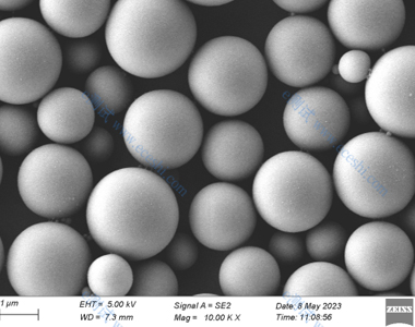
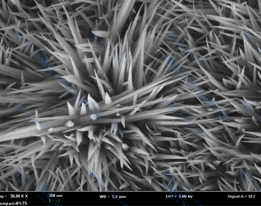
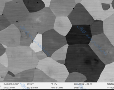
SEM/EDS Testing Services combine the high-resolution imaging capabilities of Scanning Electron Microscopy (SEM) with the elemental analysis prowess of Energy Dispersive Spectroscopy (EDS) to provide a comprehensive microstructural and compositional characterization of materials. By utilizing a focused high-energy electron beam to scan sample surfaces, SEM captures detailed topographical and morphological images, while the integrated EDS detector simultaneously identifies and quantifies the elemental composition of the analyzed micro-region. This synergistic approach delivers both visual and chemical insights at the micro- and nano-scale, making it one of the most powerful and widely used analytical techniques across materials science, electronics, and industrial quality control.
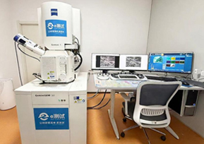
SEM/EDS Testing Services
SEM/EDS Testing Services combine the high-resolution imaging capabilities of Scanning Electron Microscopy (SEM) with the elemental analysis prowess of Energy Dispersive Spectroscopy (EDS) to provide a comprehensive microstructural and compositional characterization of materials.
Project Introduction
Application Domain
Semiconductors & Electronics
Failure Analysis: Locating chip shorts, open circuits, electromigration, and solder joint defects (voids, IMC growth).
Process Control: Measuring thin film thickness, line widths, and photoresist morphology.
Material Verification: Analyzing interface reactions and packaging material composition.
New Energy & Battery Materials
Electrode Analysis: Observing particle morphology, coating uniformity, and surface cracks.
Failure Research: Analyzing SEI film evolution, lithium plating, and separator pore blockage.
Quality Control: Screening for magnetic foreign particles (Fe, Cu) in cathode/anode powders.
Metals & Metallurgy
Fractography: Identifying fracture modes (ductile/brittle/fatigue) and origins via dimples or striations.
Microstructure: Analyzing grain boundaries, non-metallic inclusions, and alloy segregation.
Corrosion & Wear: Identifying corrosion products and evaluating coating wear mechanisms.
Polymers & Composites
Interface Analysis: Evaluating filler dispersion and fiber-matrix bonding in composites.
Aging Study: Observing surface cracking and additive migration under heat/light stress.
Film Inspection: Measuring multi-layer thickness and detecting delamination.
Biomedical & Medical Devices
Implant Characterization: Assessing surface roughness, micro-structures, and coating integrity.
Biocompatibility: Observing cell adhesion, spreading, and biofilm formation.
Cleanliness Control: Detecting particulate contaminants on device surfaces.
Geology, Mining & Environment
Mineral Identification: Rapidly identifying mineral types and analyzing ore grades.
Pollutant Tracing: Analyzing PM2.5/PM10 morphology and heavy metals in soil/water.
Microplastics: Observing morphology and assisting in polymer identification.
Archaeology & Forensics
Relic Authentication: Analyzing ancient alloy compositions, ceramic glazes, and gemstones.
Criminal Evidence: Identifying gunshot residue (GSR), paint fragments, and fibers.
Fire Investigation: Distinguishing primary vs. secondary short-circuit melting marks.
Results Display