
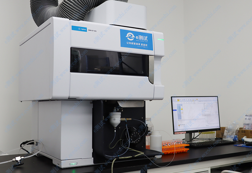
Auger Electron Spectroscopy (AES) Lab Services

Professional testing services and technical solutions for your project.

Auger Electron Spectroscopy (AES) Lab Services

Auger Electron Spectroscopy (AES) Lab Services

Auger Electron Spectroscopy (AES), also known as Auger Electron Spectroscopy, is a highly sensitive surface analysis technique based on the Auger effect. It can obtain the elemental composition and chemical state information of the topmost atomic layers (typically 0.5-10 nm) of a material surface, with a detection limit as low as 0.1 at% (atomic percent), and is capable of qualitatively detecting all elements except hydrogen (H) and helium (He) (from lithium to uranium).

Project Introduction

Auger Electron Spectroscopy (AES) Lab Services

Auger Electron Spectroscopy (AES), also known as Auger Electron Spectroscopy, is a highly sensitive surface analysis technique based on the Auger effect. It can obtain the elemental composition and chemical state information of the topmost atomic layers (typically 0.5-10 nm) of a material surface, with a detection limit as low as 0.1 at% (atomic percent), and is capable of qualitatively detecting all elements except hydrogen (H) and helium (He) (from lithium to uranium).

Service Capabilities

Surface Elemental Qualitative and Semi-Quantitative Analysis: Identifies the types of elements present on the material surface and calculates their relative content (wt% or at%) using the Relative Sensitivity Factor (RSF) method.

Micro-area Comprehensive Analysis: Possesses nanoscale spatial resolution (up to 4-10 nm), supporting point analysis, line scanning, and area scanning (Mapping) to simultaneously acquire micro-area morphology, element types, content, and two-dimensional distribution information.

Depth Profile Analysis: Combined with argon ion sputtering/etching technology, it sequentially peels off the material surface layer by layer to analyze the distribution changes of elements and chemical states along the depth direction (from a few nanometers to hundreds of nanometers).

Chemical State Analysis: Analyzes the chemical binding state, valence state, and electronic structure information of elements through the shift of Auger peak positions and changes in peak shapes.

Application Domain

Semiconductor and Microelectronics: Failure analysis of devices, analysis of tiny contaminants and defects on chip surfaces, characterization of thin film chemical components, purity and uniformity, and research on interface reactions and interdiffusion mechanisms.

Thin Film and Multilayer Film Materials: Determination of film thickness, interface diffusion width, and diffusion mechanisms, applicable to passivation films, thermal barrier coatings, ferroelectric films, hard films, etc.

New Energy and Lithium Battery Materials: Research on the composition and structural evolution of the Solid Electrolyte Interface (SEI) film, lithium distribution and embedding mechanism of negative electrode materials, and analysis of active substance distribution and failure mechanisms of electrode materials.

Metal Materials and Corrosion Research: Analysis of grain boundary embrittlement of metals and alloys, surface segregation after pressure processing and heat treatment, surface corrosion mechanisms, and detection of micro-area pollution on bulk samples.

Nanomaterial Characterization: Analysis of surface dopant enrichment layers of nano-ceramic powders, and composition analysis of nanoparticles and nanotubes.

Need a quick test for your materials?

Drop your requirements here and get a response within 24 hours.

Contact Us