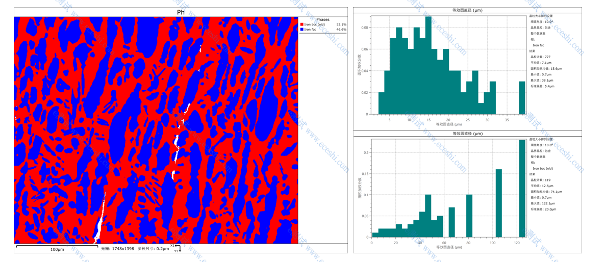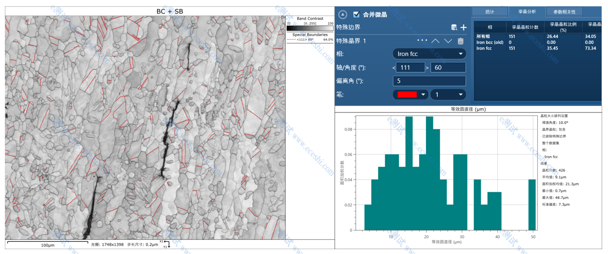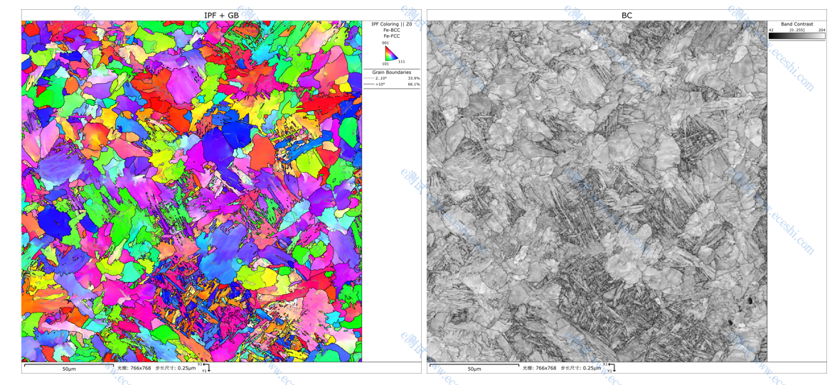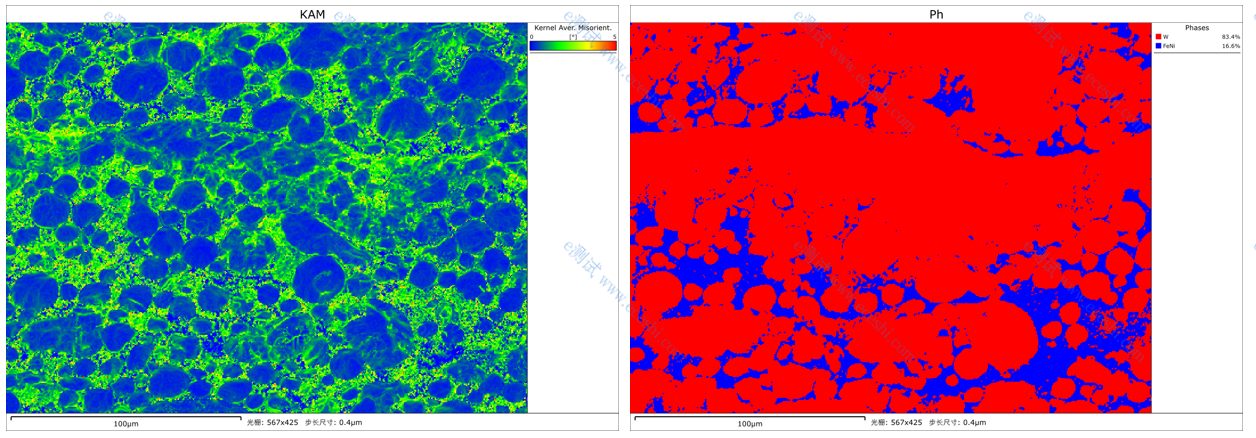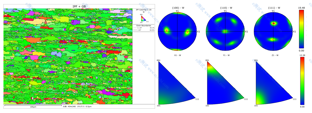
EBSD uniquely combines the conventional capabilities of Scanning Electron Microscopy (SEM) with sub-micron spatial resolution diffraction. It serves as a powerful analytical tool for rapid and accurate crystal orientation measurement. Its primary applications include the measurement of orientation and misorientation, microtexture analysis, phase identification, as well as strain and true grain size measurement.
Sample Requirements
1. Dimensional Requirements:
Sample dimensions must not exceed 25 mm in diameter and 10 mm in thickness. The optimal size ranges from 7×7 mm to 10×10 mm, with a recommended thickness of 1–3 mm. Excessively large samples increase the distance to the detector and require a higher Working Distance (WD), which reduces the pattern indexing rate and significantly increases the likelihood of sample drift during EBSD acquisition.
2. Sample Preparation Requirements:
Samples must be conductive. Mounted samples can be electrically connected to the stub using conductive adhesive, while non-conductive specimens require gold or carbon coating. Mechanical polishing must be performed prior to any final preparation steps, such as electrolytic polishing, vibratory polishing, or argon ion milling.