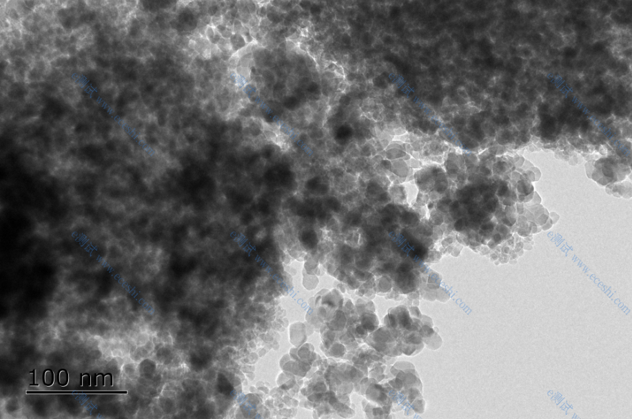
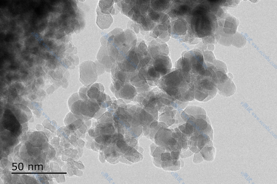
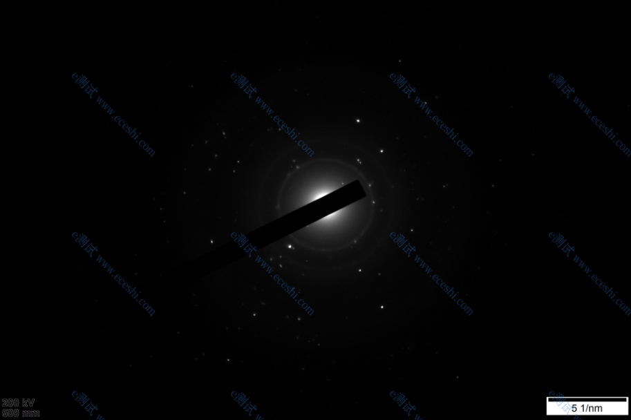
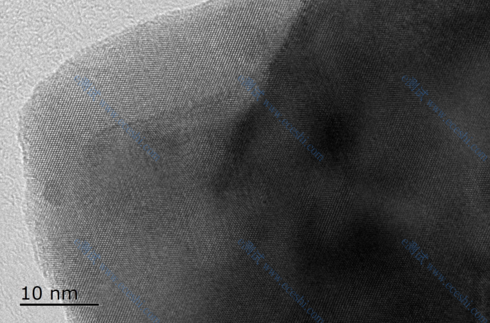
Transmission Electron Microscopy (TEM) Lab Services provide atomic-scale microstructural and compositional characterization by directing a high-energy electron beam through ultra-thin specimens (<100 nm). With resolution reaching 0.1–0.2 nm—hundreds of times beyond optical microscopy—TEM is the definitive tool for visualizing internal structures, crystal defects, interfaces, and elemental distributions that SEM surface imaging cannot access.
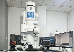
Transmission Electron Microscopy (TEM) Lab Services
Transmission Electron Microscopy (TEM) Lab Services provide atomic-scale microstructural and compositional characterization by directing a high-energy electron beam through ultra-thin specimens (<100 nm). With resolution reaching 0.1–0.2 nm—hundreds of times beyond optical microscopy—TEM is the definitive tool for visualizing internal structures, crystal defects, interfaces, and elemental distributions that SEM surface imaging cannot access.
Project Introduction
Application Domain
TEM Lab Services – Application Areas
TEM (Transmission Electron Microscopy) delivers atomic-scale imaging, crystallographic analysis, and nanoscale elemental/chemical characterization by transmitting high-energy electrons through ultra-thin specimens (<100 nm), with resolution down to 0.1–0.2 nm.
Semiconductors & Electronics
Advanced process node (≤5 nm) critical dimension measurement, gate oxide thickness evaluation, and doping distribution analysis
Multi-layer film structure and heterojunction interface characterization via HAADF-STEM Z-contrast imaging
Device failure analysis: electromigration voids, TSV/microbump defects, impurity/contamination localization
LED epitaxial structure evaluation and MEMS device microstructural assessment
Battery & New Energy Materials
SEI/CEI film composition and evolution characterization, lithium dendrite observation
Cathode/anode particle morphology, coating uniformity, and interface reaction layer analysis
Solid electrolyte ion channel mapping and structural evolution during charge/discharge (in-situ TEM)
Catalyst nanoparticle size, dispersion, active site identification, and structure–activity correlation
Nanomaterials & Advanced Materials
2D materials (graphene, TMDs) layer counting and defect analysis; quantum dot and carbon nanotube atomic structure
Metal/alloy precipitate distribution, dislocation density, grain boundary character, and phase transformation studies
Ceramic and composite interface structure, grain boundary phase composition analysis
MOF pore structure analysis and nanomaterial crystallinity evaluation
Biomedical & Life Sciences
Subcellular ultrastructure: organelles (mitochondria, ER), membrane systems, cytoskeleton
Virus particle identification, 3D structure reconstruction (cryo-EM), and vaccine/drug evaluation
Exosome/liposome/nanoparticle morphology, size distribution, and dispersion characterization
Immunogold labeling for protein/antigen localization; biological drug contamination detection (mycoplasma, viral particles) per pharmacopoeia standards
Geology, Environmental & Earth Sciences
Mineral phase identification, crystal structure, and micro-nano scale compositional analysis
Lunar/planetary sample analysis (e.g., Chang'e mission lunar regolith carbon structure and solar-wind-induced water studies)
Atmospheric particulate matter (PM2.5/PM10) morphology and source tracing
Automotive & Industrial Manufacturing
Automotive-grade semiconductor and power device microstructural qualification
Exhaust gas purification catalyst characterization
Precision component fatigue failure root-cause analysis, coating/interface integrity evaluation
Polymer, rubber, and composite material ultrastructural and filler dispersion analysis
Results Display