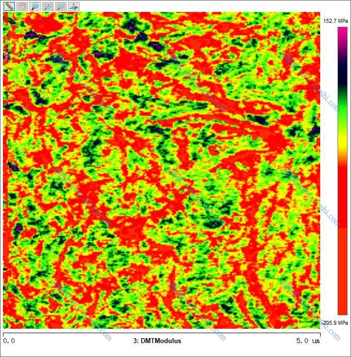
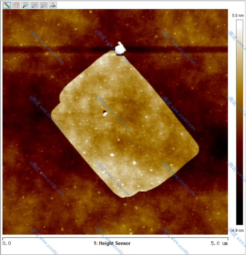
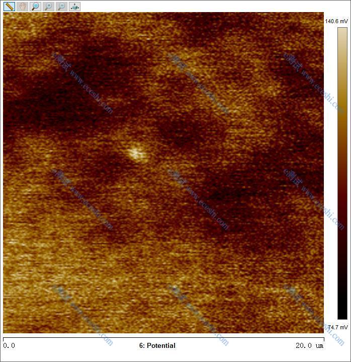
Atomic Force Microscopy (AFM) Lab Services deliver high-resolution, three-dimensional surface characterization and multi-dimensional nanoscale property mapping by detecting the weak interaction forces between a sharp micro-cantilever probe and the sample surface. Unlike electron microscopy techniques that require vacuum environments and conductive coatings, AFM operates in ambient air, liquid, or controlled atmospheres, and can directly image conductors, semiconductors, and insulators alike with sub-nanometer vertical resolution and nanometer-scale lateral resolution—making it the definitive "nanoscale tactile probe" for surface science.
Atomic Force Microscopy (AFM) Lab Services
Atomic Force Microscopy (AFM) Lab Services deliver high-resolution, three-dimensional surface characterization and multi-dimensional nanoscale property mapping by detecting the weak interaction forces between a sharp micro-cantilever probe and the sample surface.
Project Introduction
Application Domain
AFM Lab Services – Application Areas
AFM provides 3D nanoscale surface topography plus mechanical, electrical, and magnetic property mapping—operating in air, liquid, or controlled environments without requiring conductive coatings.
Semiconductors & Electronics
Wafer surface roughness, step height, and critical dimension measurement
Thin-film thickness, uniformity, and defect inspection
Local electrical property mapping (surface potential, conductivity, doping distribution)
Energy & Battery Materials
Electrode surface morphology and SEI/CEI film characterization
In-situ observation of electrode changes during charge/discharge
Photovoltaic material surface potential and grain boundary analysis
Nanomaterials & Polymers
2D material (graphene) layer counting and defect detection
Polymer blend phase separation and nanomechanical property mapping (modulus, adhesion)
Coating pinhole detection and thickness uniformity evaluation
Biomedical & Life Sciences
Live-cell imaging in liquid environment (migration, division, morphology dynamics)
Biomolecule (DNA, protein) structure and single-molecule force measurement
Virus, exosome, and nanoparticle morphology/size characterization
Magnetic & Ferroelectric Materials
Magnetic domain imaging (MFM) for storage media and spintronic devices
Ferroelectric domain structure and piezoelectric response mapping (PFM)
Nanofabrication
AFM-based nanolithography for prototype patterning and surface modification
Results Display